-:Logic gates:-
Basic gates:-
There
are
three basic gates in digital electronics. These are NOT gate, AND gate & OR
gate.
NOT gate / Inverter :-
NOT gate
is called inverter also. Operation of NOT gate is if input is high output is
low and if input is low then output is high. Another words output is always
inverse or toggle of input. So it is called inverter. Circuit diagram of
inverter is given below
Here input is A output :-
Truth table of NOT gate:-
From truth
table we can say that NOT gate shows output high if the input low and shows
output low if the input high. Example: A is an input signal for
NOT gate in black color and X is the output signal in red color. It is clear
NOT gate always reverses its input signal.
Truth table of NOT gate:-
Truth table of NOR gate:-
OR Gate:-
The output
is high if any input is high for OR gate operation. Only output is low when all
input is low. If input A, B and output is X. Then the operation is written in
with plus (+).
Mathematically
X = A+B.
Symbol of OR Gate:-
Truth table of OR gate :-
Here two
inputs are shown in the table. For first case where two inputs are low, output
also low. But all outputs are high because any one input is high. Example: A
and B are the input here. If one input is high then output is high. Output wave
X shows that.
Truth table of OR gate:-
AND gate:-
When all
inputs are high output is high in AND gate. If one input is low then output
low. Diagram of AND gate is
Symbol
of AND Gate:-
Truth table of AND gate:-
AND
operation is written multiple with the inputs. For input A, B and output X the
operation is X=AB or X=A.B Example: From output signal where the two
inputs are high output also high. Otherwise all area are low in AND gate.
Truth table of AND gate:-
NOR Gate:-
NOR gate
is opposite of OR gate. NOR gate gives high output when all inputs are low.
Diagram of NOR gate approximately same only one change that a single bubble
used in output bar.
Symbol
of NOR Gate:-
Truth
table shows
only when all inputs are low then output high. Example: NOR gate
produces low when any one of input is high.
NAND Gate:-
NAND gate
also opposite of AND gate. NAND gate produces high if all input are low
otherwise all output are high. Diagram of NAND gate similar to AND gate only
one change that is one bubble used to output terminal.
NAND
operation written in:-
Truth table:-
XOR Gate:-
XOR gate
means exclusive OR gate. When both inputs are opposite logic level only then
output are high.
Expression
of XOR gate written as alternatively written:-
Truth table:-
Logic Families:-
•Logic Family : A collection of different IC’s that
have similar circuit characteristics.
•The circuit design of the basic gate of each logic
family is the same.
•The most important parameters for evaluating
and comparing logic families include :
–Logic
Levels.
–Power
Dissipation.
–Propagation
delay.
–Fan-out
( loading ).
Example Logic Families:-
Example Logic Families:-
•General
comparison or three commonly
available logic families.
Implementing
Logic Circuits:-
• There
are several varieties of transistors –
the building blocks of logic gates – the
most
important are:
–BJT (bipolar junction transistors)
•one of the first to be invented
–FET (field effect transistors)
•especially Metal-Oxide
Semiconductor
types (MOSFET’s).
•MOSFET’s are of two types: NMOS
and PMOS.
TTL
and CMOS:-
•Connecting
BJT’s together gives rise to a
family of logic gates known as TTL.
•Connecting
NMOS and PMOS transistors
together gives rise to the CMOS family of
logic gates.
Electrical Characteristics:-
•T T L
–faster (some versions).
–strong drive capability.
–rugged.
•C M O S
–lower power consumption.
–simpler to make.
–greater packing density.
–better noise immunity.
•
Complex IC’s contain many
millions of transistors.
• If
constructed entirely from TTL
type gates would melt.
• A
combination of technologies
(families) may be used.
• CMOS
has become most popular
and has had greatest development.
Logic Level & Voltage Range:-
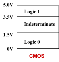
•Typical
acceptable voltage ranges for
positive logic 1 and logic 0 are shown
below.
•A
logic gate with an input at a
voltage level within the
"indeterminate" range
will produce
an unpredictable output level.
Characteristics:
TTL and MOS:-
Remember:-
•TTL
stands for Transistor-Transistor Logic.
–uses
BJTs.
•MOS
stands for Metal Oxide
Semiconductor.
–uses
FETs.
•MOS
can be calassified into
three sub-
families :-
–
PMOS (P-channel).
–
NMOS (N-channel).
–
CMOS (Complementary MOS, most common).
Transistor-Transistor
Logic Families:-
•Transistor-Transistor Logic Families:
–74L Low
power
–74H High
speed
–74S Schottky
–74LS Low
power Schottky
–74AS Advanced
Schottky
–74ALS Advance
Low
power Schottky
CMOS
Logic Families:-
•CMOS
Logic Families
–40xx/45xx Metal-gate
CMOS.
–74C TTL-compatible CMOS.
–74HC High speed CMOS.
–74ACT Advanced CMOS -TTL
compatible.


إرسال تعليق
Welcome to BishwasEducation